
GENUINE TOYOTA SPARE PARTS
View a selection of our most popular car parts
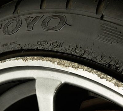
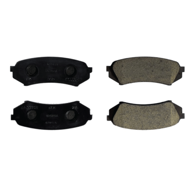
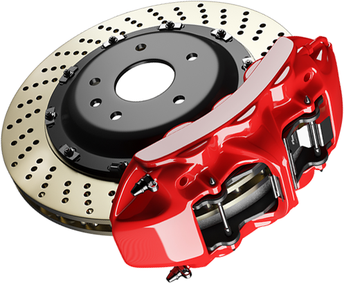
Popular
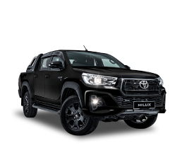
Featured
New arrivals
Customers Rate us 4.7 / 5
Check our latest reviews from customers


DAKS TOYOTA News & Blogs
Check our latest news, events & blogs
View a selection of our most popular car parts
Check our latest reviews from customers
Check our latest news, events & blogs